Crack open any electronics device and you’ll find a host of tiny components within. Manufacturing these connectors and shields is complex work, far more challenging than the stamping, bending, and machining performed on much larger parts. For one thing, the individual features on these micro-sized components are often just a human hair-width or two across. The materials are equally thin, ranging from 0.001″ to 0.032″ (0.025 to 0.813 mm) in thickness—in many cases, it’s like trying to cut a complex shape the size of a pencil eraser or smaller from a piece of aluminum foil.
And because the electronics industry continues to evolve and products grow more capable, interconnected, and above all, wireless, these parts will only grow smaller over time. The result? The people developing these products will need the ability to quickly test multiple prototypes and small lot runs before arriving at an optimal design, long before they have to invest in a dedicated progressive die.
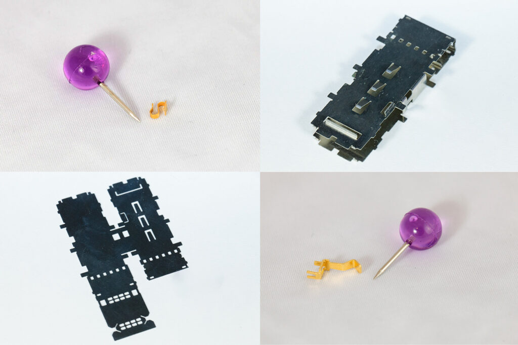
The good news is there’s a manufacturing technology able to deliver just that. At Createproto, we like to call it Rapid Micro Stamping™ (RMS). You might also hear it referred to as Small Metal Stamping, Thin Gauge Metal Stamping, Micro Miniature Metal Stamping, or Precision Micro Stamping, among others. Although none of these names fully encompasses all the various processes used, RMS is to the electronics industry what 3D printing and other rapid prototyping methods are to other industries. RMS provides extremely quick turnaround, significant design flexibility, and cost-effective manufacturing of even low quantities, often serving as a bridge between the design and ramp-up phases and full-blown production.
RMS works by mimicking the multiple stages found in a progressive die. Instead of building a tool that takes raw material in one end and spits out finished parts at the other, RMS splits the stamping, forming, punching, and other operations of a “prog” die into discrete steps. These steps are typically performed on manual equipment, assembly line fashion, giving original equipment manufacturers (OEM) and electronic manufacturing services (EMS) companies the ability to order tens or perhaps thousands of parts with minimal investment and receive them in record time.
So why is it needed? If you haven’t yet ditched your telephone landline, chances are good that you hear an annoying hiss from time to time while talking to your Aunt Betty. It’s caused by a phenomenon known as electromagnetic interference (EMI), or sometimes its smaller, more range-specific subset, radio frequency interference (RFI). Whatever the origin, it’s why the flight attendant on the trip to Boise last month told you to turn off everything but your small electronics during the takeoff and landing, as the slight amount of EMI emitted by laptop computers is supposedly enough to interfere with the navigation systems.
On a larger scale, EMI is caused by lightning storms, solar flares, power lines, and electrically noisy appliances like power tools and clothes dryers. Fortunately, we don’t notice it much because electronics designers do a darned good job of shielding our smartphones and laptop computers from such wayward electromagnetic radiation.
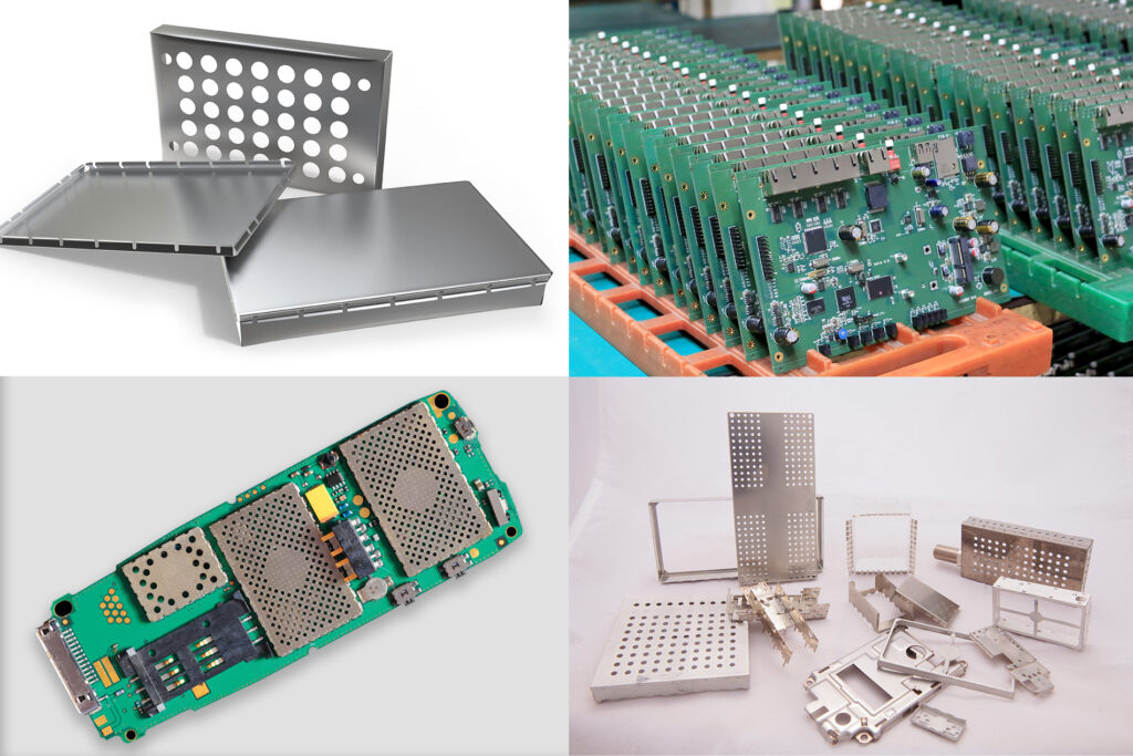
However, as these and other devices grow more compact and the printed circuit boards (PCBs) within become crammed with an increasing number of electronic widgets, board level shielding (BLS) gets even more important. At its basic level, BLS entails shielding an individual component or a group of components on the board, though there are plenty of variations. There are 3 distinct types of BLS: 1-piece shielding cans, 2-piece shielding cans, and multi-cavity shields. With 1-piece shielding, you have one stationary piece, which stays put once mounted. With 2-piece shielding, the top or cover is a separate piece, and is removable to facilitate quick repairs on the component underneath. Finally, for maximum savings of your valuable board real estate, you’d use a multi-cavity shield which reduces or eliminates the adjacent mounting edges that would be needed with multiple contiguous single-component shields. Mounting presents additional options: any of the three types of BLS can be mounted either by way of surface mounting, which uses a full-edge solder, or through-hole mounting, in which pins are fastened into the board. Complicating matters further, any type of shield may require vent holes for air flow and heat dissipation, deep drawn or bent regions, or other custom options.
Electronic manufacturers need more than good shielding, however. With tiny circuit boards comes the need for ever smaller, thinner, and more accurate micro parts. These include grounding clips, battery contacts, lead frames, encoder discs, SFP cages, electronic contacts, terminals, filters, connector bodies, antenna elements, spring clips, ESD clips, heat sink clips, fiber optic shields, connector shields, I/O shields, and too many more to list. These micro parts are used in everything from microwave antennae to the circuit boards used in the slot machines at the local casino.
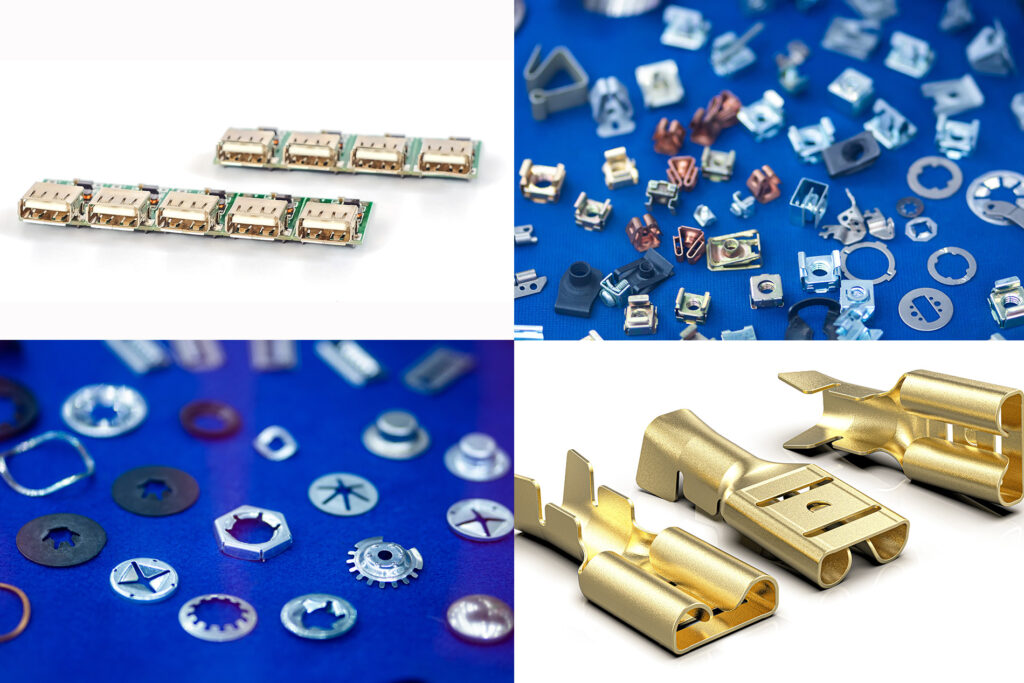
Practically all of them are made from metals such as phosphorus bronze, nickel, silver, beryllium copper (BeCU), cold rolled steel (CRS), stainless steel, copper, MuMetal, brass, and more, metals that are both wear-resistant and electrically conductive. To increase one or both these properties, they can be pre- or post-plated with tin, gold, nickel, silver, palladium, zinc, and similar elements and alloys.
PICK A PROCESS
So why does the name fall short in accurately representing how the parts are made? Even though RMS relies heavily on traditional, albeit far smaller, stamping tools and presses, it also utilizes other processes such as wire EDM, laser cutting, and especially photo etching, also known as metal etching, chemical etching, or photo chemical machining (PCM), to manufacture flat blanks, and sometimes individual components. And as mentioned earlier, RMS relies heavily on manual “one process at a time” manufacturing methods, eliminating the need for more expensive progressive tooling.
PCM is much like that used to manufacture integrated circuits, where chemicals are used to “eat away” everything that doesn’t belong on the finished part. It works by coating both sides of a metal blank with a light-sensitive polymer known as photoresist. Using a negative mask of the finished workpiece, ultraviolet light is used to selectively harden or “cure” the sections that should remain. Acid is then applied to the blank, eating away the areas in between the cured photoresist and leaving a highly accurate, burr-free workpiece behind.
It sounds like an improbable process, but has been used for decades to quickly and cost-effectively produce all manner of flat sheet metal components that can then be bent or formed into three-dimensional shapes.
ON THE TIGHT-WIRE
There’s also wire EDM, short for electrical discharge machining. As its name implies, an electrically charged “moving wire” just a few hair-widths in diameter (typically 0.008″ to 0.012″) is used to remove metal like the world’s tiniest cutting tool. Here, a workpiece blank is clamped in the machine and the wire is driven through metal under computer control, tracing the desired part shape.
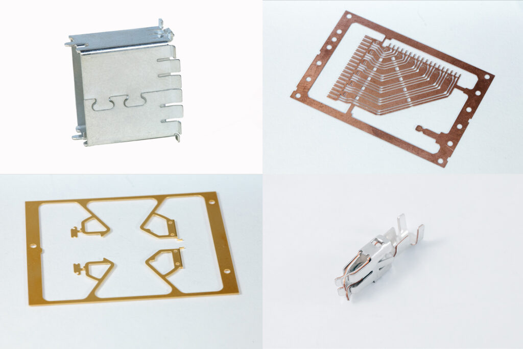
As with PCM, parts made with wire EDM are extremely accurate and burr-free, and because the metal blanks can be stacked one atop the other many inches high, tens or perhaps hundreds of workpieces can be produced in a single operation. Again, the finished part profiles may require bending or forming in a separate machine to achieve the desired three-dimensional shape, but the process is far less expensive than the alternative—a dedicated progressive die.
A laser cutter might be used in the same manner (although without the stacking just mentioned), but this would primarily be on thicker metals able to withstand the intense heat of a high-powered laser without distorting. And finally, traditional stamping techniques, described in our “What is Stamping?” blog here, are also an important part of any RMS offering, but at a much smaller scale.

